Vivado®2020.2でZynq® UltraScale+™ MPSoC Verification IP (VIP)を利用したシミュレーション(発展編②)~AXI CDMAエンジンの駆動&割り込み検出:サンプルデザインあり~
今回は前編で使用したデザインにAXI-CDMAを追加し、割り込みを使用するサンプルデザインの作成と、Zynq® UltraScale+™ MPSoC Verification IPを用いた割り込み検出を含めたAXI CDMAシミュレーションを行います。
なお、本篇で使用したEXAMPLEデザインはダウンロードできるよう準備していますので、気になる方はダウンロードしていただければと思います。あわせてご確認ください。
それでは、始めましょう。
このブログは「FPGA設計ブログ一覧」の
2. シミュレーションのひとつです。
目次
はじめに
今回使用するZynq® UltraScale+™ MPSoC Verification IP APIは以下になります。
APIの全リストは、DS941を参照ください。
DS941:Zynq UltraScale+ MPSoC Verification IP
| APIs | Inputs | Outputs |
|---|---|---|
| set_debug_level_info When set to value '1 ', debug level info for Zynq UltraScale+ MPSoC VIP is reported, else no info is reported. The default value is 1. |
LEVEL: A bit input for the info level. | None |
| set_verbosity When set to default value '32'd400', debug level info from Xii VIP is reported, else no info is reported. |
VERBOSITY:32'd0: None 32'd400: Full |
|
| pre_load_mem Preload DDR/OCM with random_data/all_zeros/all_ones. Based on the address specified, the data is loaded in DDR/OCM. DDR: Address must be 32-bit aligned. OCM: Address must be 32-bit aligned. |
[1:0] data_type:Random, zeros or ones. 1 - Random 2 - Zeros, 10 - Ones, 11 - Random [31:0] start_addr:Start Address from where DDR should be initialized with data from the file. no_of_bytes:Number of data bytes to be loaded |
None |
| read_burst Initiate a single AXI Read burst transaction on the master port. This is hook to call the AXI VIP API. This task returns when the complete read Transaction is complete. |
ADDR:Read Address (aligned address) LEN:Burst Length SIZE:Burst Size BURST:Burst Type LOCK:Lock Type CACHE:Cache Type PROT:Protection Type |
DATA:Valid data transferred by the slave RESPONSE:This is a vector that is created by concatenating all slave read responses together (maximum - 256 bytes) |
| write_burst_strb Initiate a single AXI write burst transaction on the master port with strobe control. This is hook to call the AXI VIP API. This task returns when the complete write transaction is complete. |
ADDR:Write Address LEN:Burst Length SIZE:Burst Size BURST:Burst Type LOCK:Lock Type CACHE:Cache Type PROT:Protection Type DATA:Data to send STRB_EN:1 to enable 0 to disable STRB:Strobe of Data to Send DATASIZE:The size in bytes of the valid data contained in the input data vector(maximum - 256 bytes). |
RESPONSE: The slave write response from the following:[OKAY, EXOKAY, SLVERR, DECERR] |
| wait_interrupt Use this API to wait for any of the interrupt to occur. This is a blocking task to wait for an interrupt to occur and returns immediately with any of the four interrupt lines asserts. |
[3:0] irq:Interrupt line number | [15:0] irq_status:Interrupts generated by PL. |
出典:DS941:Zynq UltraScale+ MPSoC Verification IP
https://docs.amd.com/v/u/en-US/ds941-zynq-ultra-ps-e-vip
サンプルデザインの作成手順
| 1. | 以下のコードをダウンロードしてください。 ダウンロードはこちら コードをすべて選択し、ファイル名をdesign_1.tclとして保存します。 (全部で1,829行があり、1,829行目がcreate_root_design ""であることを確認してください) |
| 2. | vipbase1のフォルダを作成し、1で作ったdesign_1.tclをvipbase1フォルダに保存します。 |
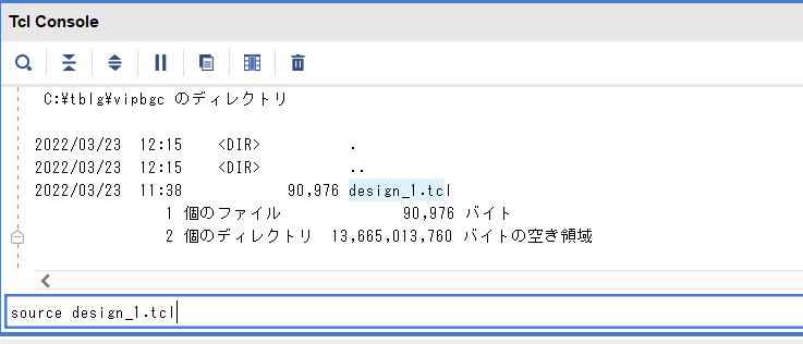
| 3. | Vivado®2020.2を起動します。tcl consoleで2にて作成したvipbase1フォルターに移動して、source design_1.tclを入力し、tclを実行します。(BDデザインを作成します) |
|
出典:Vivado® ML Edition |
|
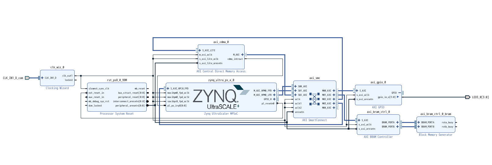
| 以下のようなデザインが作成されることを確認します。 | |
|
※画像クリックで大きな画像が表示されます。 Design_1.tclから作成されたBDデザイン 出典:Vivado® ML Edition |
|
サンプルテストベンチの作成手順
| 1. | 以下のコードをダウンロードしてください。 ダウンロードはこちら コードをすべて選択し、ファイル名をsim_tb_top.svとして保存します。 |
| 2. | Vivado®2020.2を起動し、基本編で作成したPROJECTを開きます。 |
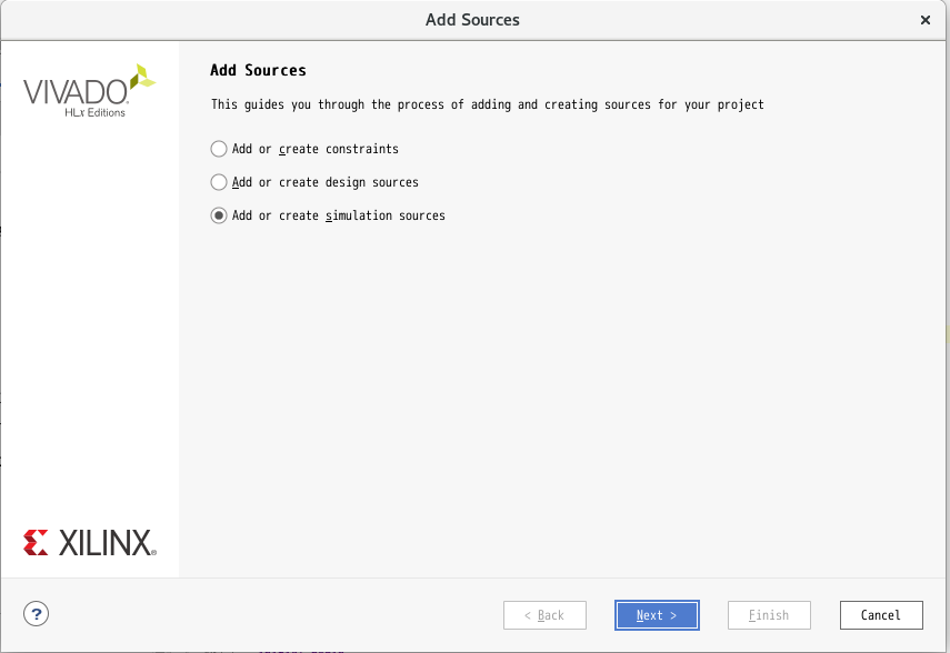
| 3. | File→Add Sources で下記のようにsim_tb_top.svをPROJECTに追加します。 |
|
出典:Vivado® ML Edition |
|
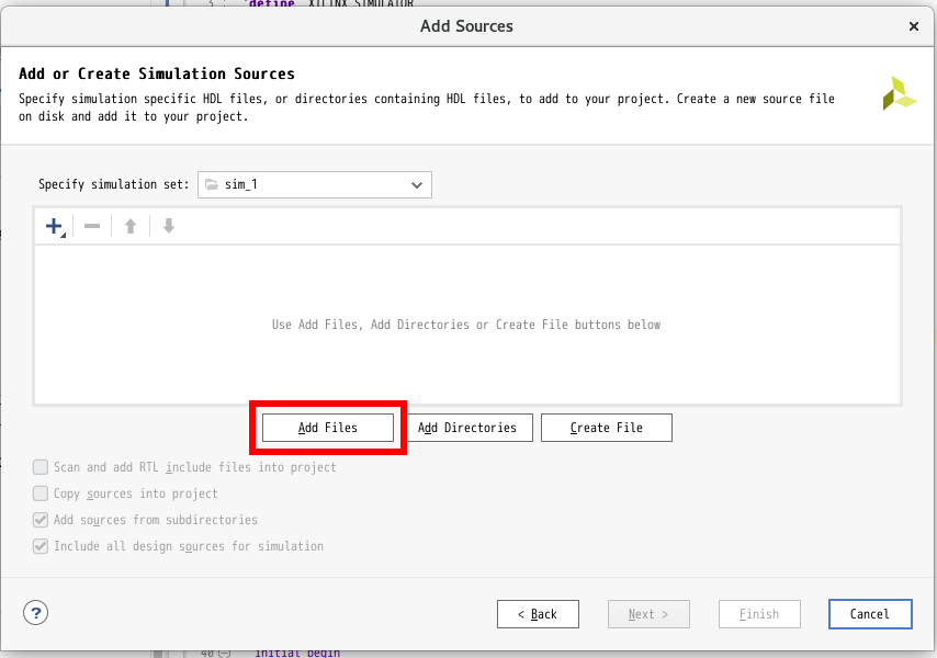
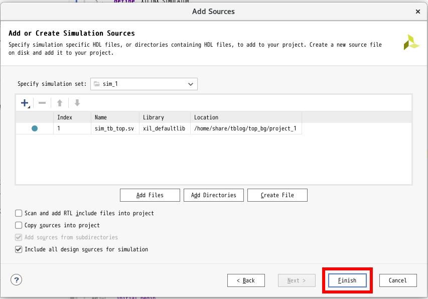
| 4. | Add Filesを選択し、sim_tb_top.svを追加します。 |
|
出典:Vivado® ML Edition |
|
| 5. | Finishを選択し、終了します。 |
|
出典:Vivado® ML Edition |
|
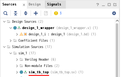
| 6. | Sourcesタブで、下図のようにsim_tb_topがtopデザインになっていることを確認します。 |
|
出典:Vivado® ML Edition |
|
シミュレーションの実行
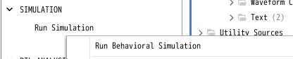
下図のようにSIMULATION→run Simulation→Run Behavioral Simulationを選択、simulationを実行する。
(環境依存で、時間がかかる場合があります)
出典:Vivado® ML Edition
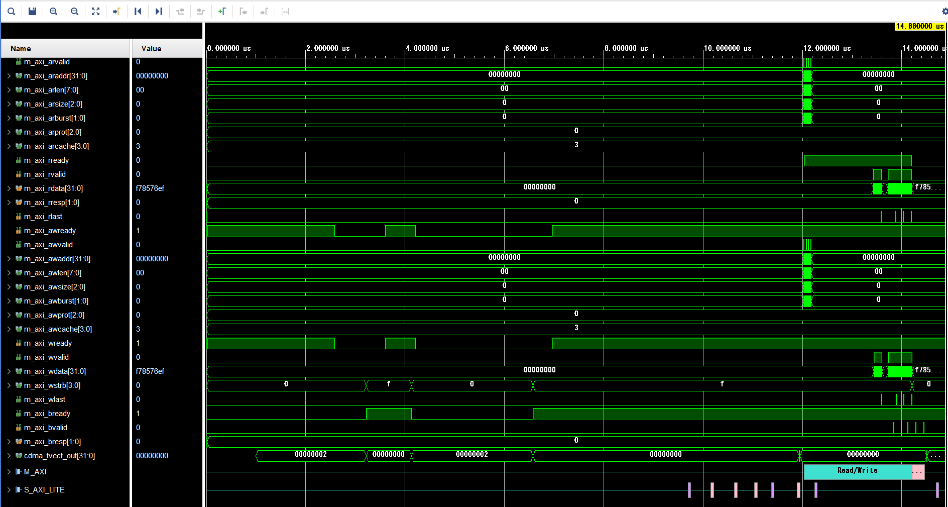
観測したい信号を追加し、runを再実行して、波形を観測します。(4つのLEDが順番に動作していることを波形上で確認できます)
出典:Vivado® ML Edition
シミュレーション結果はTcl console上でも確認ができます。
SUCCESS: CDMA interrupt receivedとTestbench finished の行で確認します。
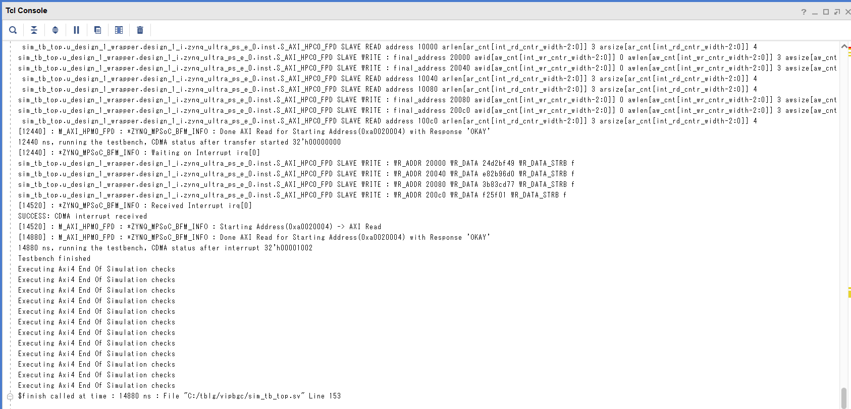
出典:Vivado® ML Edition
EXAMPLEデザイン
本ブログでは、PL側のDMAを用いたVIPシミュレーションの方法を紹介しました。
EXAMPLEデザインについては以下よりダウンロードいただけます。
おわりに
いかがでしたでしょうか。これでVIPも用いたシミュレーションが実行できました。
次回はDUAL VIPを利用したシミュレーションの方法を紹介したいと思います。
最後までご覧いただきありがとうございました。
このブログは「FPGA設計ブログ一覧」の
2. シミュレーションのひとつです。
参考資料:
DS941:Zynq-7000 All Programmable SoC Verification IP v1.0
Xilinx Answer 69622
Xilinx Answer 70185
Xilinx Answer 70186
Xilinx Answer 75942